-
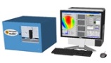
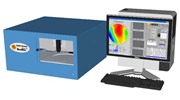
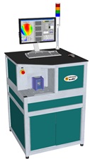
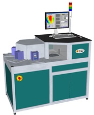
System platform: desktop or standalone.
-
Wafer loading: desktop: manual; standalone: manual or automated.
-
Wafer size: desktop: 2", 3", 4" (options: any size up to 8" or 12"); robot system: 2"-6" (with potential to 8 inches).
-
System test functions: EL, PL, EL/PL combination, IV, reverse, warpage, film thickness, etc.
-
Probe type: Type I, Type IA, Type II, Type IIA, Type IIB, Type IIC, and Type SiA.
-
Targeted material: LED epiwafers, nearly any type of semiconductor-based light-emitting material systems.
EpiEL mapping system has been
extensively tested on nitride-based material systems; please check with MaxMile for other types of material systems.
-
Light detection: standard for transmission mode; reflection
mode will be optional (for samples with opaque substrates).
-
Test mode: quick or mapping.
-
EL test protocol: curve or point.
-
Test speed: 0.5-12 minutes, depending on test functions and their configurations.
-
Sampling points: number of sampling points and
optical/electrical measurements for each point can be specified by
end user. User can generate own test point arrangement.
-
Wavelength detection: UV/VIS/NIR, or customized range.
-
Spectral resolution: 0.5-2 nm, depending on spectral range configuration.
-
Excitation sources:EL: electrical; PL: 405nm standard, please contact MaxMile for other excitation sources.
-
Current measurement: >10e-12A.
-
Type of curves: Characterizations provided by MaxMile EpiEL systems.
-
Type of mappings: Characterizations provided by MaxMile EpiEL systems.
-
Mapping color encoding: rainbow, gradient,
binary, temperature, gray, or any type specified by end user.
-
Report generation and data presentation: HTML (Brief/Abbreviated/Full), XML, CSV, TXT (Each kind of report is configurable. Software can be customized to meet specific report need).
-
Control unit and OS: PC-based EpiEL station run on MS Windows 7 (32bit or 64 bit).
-
Power supply: 20A/110VAC or 10A/220VAC; Vacuum needed for robot system.
-
Recommended Ambient Condition: temperature: 15'C-30'C, humidity: 40%-70% without condensation.
-
Other robot system features: wafer alignment: yes; cassette wafer mapping: yes; cassette auto check: yes.
-
System Dimension: desktop: 4 inches: 18"(w)x18"(d)x14"(h), 8 inches: 24"(w)x24"(d)x14"(h); robot system: MaxMile robot: 32"(w)x32"(d)x68"(h); commercial robot: 57"(w)x32"(d)x68"(h).
-
Options: EpiEL station: desktop or standalone; Size of desktop EpiEL station: 4 or 8 inches; Robot configuration: commercial or MaxMile; Dual EL detection (EpiEL-700); PL Option; Film thickness, etc. (Note: warpage and reverse test will be a standard configuration of EpiEL system).