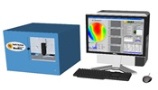
Desktop 4 Inches
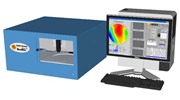
Desktop 8 Inches
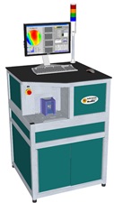
Robot I
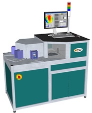
Robot II
|
|
|
|
|
| |
|
Typical Characterizations Provided by MaxMile EpiEL, PL, and EL/PL combination Systems
MaxMile's EpiEL, PL, and EL/PL combination
mapping systems have the capabilities to rapidly determine the
device-level emissive and electrical properties of light-emitting
materials without device fabrication. They can be used either as (a) a
wafer-scale mapping test, or (b) a quick test tool for random and
individual point test.
|
|
Quick Test
In quick test mode, full-scale emissive and electrical properties of light-emitting
materials can be nondestructively characterized at preconfigured points or at any point within the
wafer, which include:
- EL spectra at specific driving current/voltage
- PL spectrum
- LIV---current-voltage and emission-voltage characteristics
- Output intensity characteristics
- Wavelength (WLP, WLD, or WLC) & FWHM vs. driving current
- Reverse IV
|
|
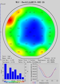
Wafer-scale Mapping Test
MaxMiles proprietary EpiEL
probe technology ensures that the above device-level emissive and
electrical characterization can be reliably performed over an entire
wafer. This capability makes wafer-scale, rapid and nondestructive
EL mapping possible. After properly selecting the mapping area and
number of sampling points, various emissive and electrical mapping
will be obtained in a few minutes, which includes:
EL mappings:
- Wavelength
- WLP-peak wavelength
- WLD-dominant wavelength
- WLC-Center wavelength
- FWHM
- Blue Shift
- Blue Shift Rate
- Intensity
- Radiometric power
- Photometric power
- Slope efficiency
- etc.
- Electrical
- Measured forward voltage
- Measured forward current
- Device Vf
- Device If
- Turn-on voltage
- Threshold voltage
- On-resistance
- On-resistance NL
- Top resistance
- Forward leakage current
- Series resistance
- Ideality factor n
- Reverse leakage current
- Reverse leakage voltage
- etc.
|
IV mappings:
- Forward voltage
- Forward current
- Device Vf
- Device If
- Threshold voltage
- On-resistance
- On-resistance NL
- Top resistance
- Series resistance
- Ideality factor n
- Reverse leakage current
- Reverse leakage voltage
- etc.
PL mappings:
- Wavelength
- WLP-peak wavelength
- WLD-dominant wavelength
- WLC-Center wavelength
- FWHM
- Intensity
- Radiometric power
- Photometric power
Other mappings:
|
Usually each mapping point has following curves:
- EL spectra at specific driving current/voltage
- PL spectrum
- LIV---current-voltage and emission-voltage characteristics
- Output intensity characteristics
- Wavelength (WLP, WLD, or WLC) & FWHM vs. driving current
- Reverse IV
Note: Software can be customized for specific device parameter mapping.
|
|
|
An example of auto-generated HTML report
|
|
|
To learn more about MaxMile EpiEL, PL, or EL/PL Combination technologies:
|
|
|
|
|
|